This
section presents a simple introduction to JTAG technology.
For more comprehensive description please refer to the sites
in the section Links.
|
|
In
today's complex systems, testability is an increasing concern
in almost every application and in every area of application
development. Manufacturers that thoroughly address the issue
of testability at the device, board, and system levels deliver
more consistently reliable and cost-effective products to the
marketplace.
This means building in test capabilities in
every phase of development and deployment, including design
verification, hardware and software integration, manufacturing,
and in the field.
In
the 1980s, the Joint Test-Action Group (JTAG)
formed by representatives from makers and users of components
and boards, recognised that only a cooperative effort could
address the mounting testability problems in a coordinated
way. Its mandate was to propose design structures that semiconductor
makers would incorporate into device designs to aid in testing
boards and systems. In 1990 the IEEE adopted the proposal
as IEEE Standard 1149.1. Its stated purpose
was to test interconnections between Integrated Circuits (ICs)
installed on boards, modules, hybrids, and other substrates.
Manufacturers adopting the standard could also test the IC
itself. |
Architecture
IEEE Standard 1149.1 is a testing standard. However it is described
as a collection of design rules applied principally at the IC level
that allow software to alleviate the growing cost of designing and
producing digital systems. The primary benefit of the standard is
its ability to transform extremely difficult printed circuit board
testing problems that could be attacked with ad-hoc testing methods
into well-structured problems that software can easily and swiftly
deal with. To conform to the boundary-scan standard IEEE 1149.1,
a device must contain the following: Test Access Port
(TAP), Scannable Instruction Register,
Scannable Data Registers, TAP Controller.
|
The Boundary Scan Register and other test
features of the device are accessed through a standard interface
- the JTAG Test Access Port (TAP). According to the standard,
the TAP must contain four signals, each available through
a dedicated device pin and they may not be shared with any
other function:
- Test Data Input (TDI): it is used to shift
data and instruction tests into the Boundary Scan register.
- Test Data Output (TDO): this pin provides
data from the Boundary Scan register or other internal register.
- Test Clock (TCK): this input controls test-logic
timing independent of clocks that normal system operations
employ. The TDI shifts values into the appropriate register
on the rising edge of TCK. Selected register contents shift
out onto TDO during the TCK's falling edge.
- Test-Mode select (TMS): this input, which
also clocks through on the rising edge of TCK, determines
the state of the TAP controller.
|
|
An
optional active-low Test-Reset Pin (TRST#) permits
an asynchronous TAP controller initialisation without affecting
other device or system logic. Asserting this pin inactivates the
boundary-scan register and places the device in normal operating
mode. These
pins are used with a simple protocol to communicate with on-chip
Boundary-Scan logic.
|
Several
different data registers can be built into
boundary-scan components. All Boundary-Scan instructions set
operational modes that place a selected data register between
TDI and TDO. This register is referred to as the target register.
This preserves a fundamental notion of Boundary-Scan: TDI
and TDO always form the ends of a shift register.
The function of this register is dictated by the effective
TAP instruction.
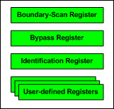
Two
Data Registers are always required to be present on a 1149.1
component: the Boundary-Scan Register and
the Bypass Register. Several others are described
by the standard, such as an Identification Register,
but are optional. |
The
Test Data Register loads the data in parallel on
the rising edge of TCK in the TAP Controller state CAPTURE-DR (triggering
test results), puts the data on the output parallel latch on the
falling edge of TCK in the TAP Controller state UPDATE-DR (new test
pattern generation), and shifts the serial data through TDI to TDO
during the TAP Controller state SHIFT-DR.
| The
TAP Controller is a 16-state finite
state machine added on the IC die itself. It recognises
the communication protocol and generates internal control signals
used by the remainder of the Boundary Scan logic. The TAP controller
is driven by TCK and TMS only; no other signals affect TAP controller.
They programme the TAP Controller as a 16-state machine, generating
clock and control signals for the instruction and data registers.
Only three events can trigger a change of controller state:
a test-clock rising edge, and system power-up.
Movement through the state machine is controlled by the value
of TMS, a set-up time prior to the rising edge of TCK. The 1s
and 0s adjacent to each state transition arc show the value
that must be present on TMS at the time of the next rising edge
of TCK.
The different state can be divided in 4 groups:
Reset, BIST, Data Register Update, Instruction Register
Update.
|
|
The Boundary-Scan
Standard allows for ICs to be linked into chains by linking the
TDO pin of one IC with the TDI pin of the next. For example, the
1149.1 ICs on a board may all be linked together by their TDO-TDI
pins in succession. Several distinct chains may exist on a board
if they do not share any TAP signals.
The
1149.1 Standard allows us to exploit the Boundary-Scan to test a
board composed of Boundary-Scan chips.
|
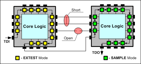
Interconnect
tests look for shorts between boundary-scan nodes and conventional
nodes with bed-of-nails or edge-connector access, as well as
opens between tester nails and boundary-scan input pins. The
EXTEST instruction latches boundary-scan nodes
to the state that permits easier in-circuit backdrive (a logic
1 to TTL). The tester then looks for node movement when it forces
non-boundary-scan nodes to their opposite states. |
Applying
this technique to a single conventional node places a 1 on that
node and scans out boundary-scan-input states, then injects a 0
onto the test node and scans again. A short between
the test node and a boundary-scan node will show up as a failure.
An open connection will cause both scanning operations
to produce exactly the same output pattern.
Some
shorts other than the one between test and boundary-scan nodes can
cause this operation to fail. Only rarely, however, will such a
faulty node follow the test node at both the latched-1 and latched-0
states. Changing test-node states several
times and declaring a short only when the suspect boundary-scan
node exactly follows these transitions further improves the likelihood
of a correct diagnosis.
|


